Flexible Printed Circuit
Flexible printed circuit boards (FPCs) are becoming increasingly important. Invented back in the 1950s, their widespread use in commercial applications began in the 1980s. In contrast to conventional, rigid printed circuit boards, the insulating layer that contains the conductive tracks and other switching elements is not made of hard plastics, but of flexible films - usually polyimides. These are characterised by high heat resistance (up to 230 °C, briefly up to 400 °C), low degassing, high radiation resistance and excellent insulating properties - ideal properties for FCBs.
Advantages of flexible printed circuit boards:
The main advantage of FPCs is their flexibility and small form factor. This enables more compact designs and makes them particularly suitable for applications with limited installation space or complex geometries. They can also be combined in several layers to form a circuit (multilayer) - even in combination with rigid layers (so-called rigid-flex PCBs).
Despite these advantages, flexible PCBs also pose challenges: Compared to conventional (rigid) solutions, FPCs are significantly more expensive and more sensitive, meaning they can be damaged more easily. These properties require specialised testing approaches.
Typical application fields for flexible printed circuit boards:
- 3C industry (computer, communication, consumer electronics): Used in smartphones, tablets, wearables, cameras, and headphones - wherever space-saving and flexibility are required.
- Automotive technology: Used in steering wheel controls, airbags, sensors, and lighting technology in modern vehicles.
- Medical technology: Used in portable devices and implants that necessitate miniaturisation and flexibility.
- Industrial electronics: Applications in machines and devices where compact, flexible designs are required.
Challenges of FPCs contacting
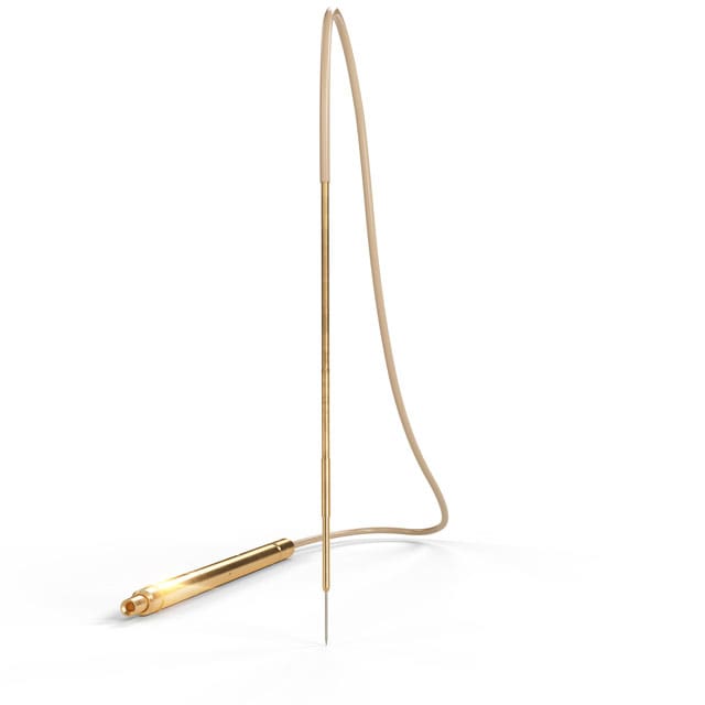
The flexibility of FPCs makes precise, reproducible contacting of the test points difficult. Due to their minimal material thickness (< 0.5 mm), spring-loaded test probes must be designed to ensure that they reliably contact the test points without damaging the FPCs - especially due to excessive spring force or aggressive tip styles.
These are particularly challenging:
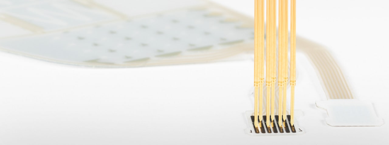
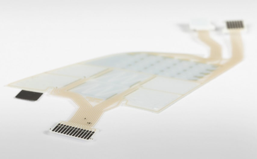
- High contact point density: Many test points on a small grid (e.g. 16 test points in a grid of only 0.5 mm) require specialised contacting solutions.
- Multilayer FPCs: If the test probe penetrates the outer layer, it can unintentionally hit underlying layers, leading to short circuits or functional failures.
- Customised test fixtures: The production of specialised test fixtures is often time-consuming and costly, especially if FPCs must be contacted from various angles because they are already connected to other electronics.
Gold finger technology for reliable contacting
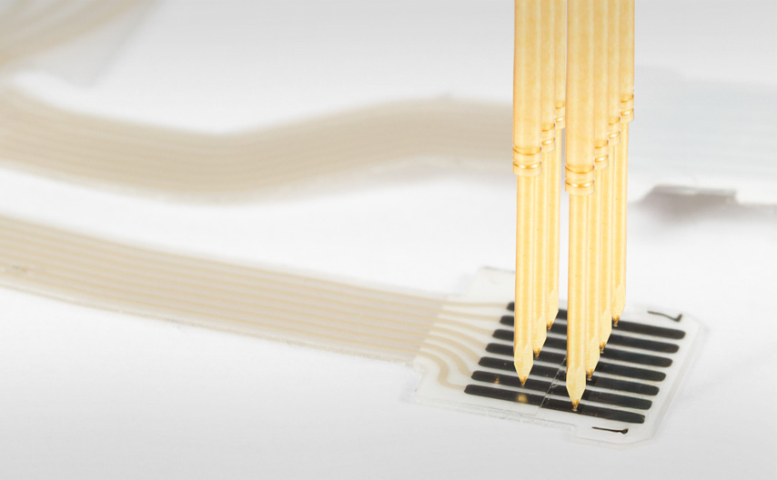
To overcome these challenges, INGUN offers specialised solutions for testing flexible printed circuit boards: FPC cables with gold fingers (contact fingers). These can be tested with spring-loaded test probes from the GKS-038, GKS-040, and GKS-069 series. The contacting is offset on the contact surfaces so that a larger grid and mechanically more durable test probes can be used. It is vital that the flexible PCB is well centred in the test fixture using a guide plate.
Penetrate OSP coatings effortlessly
The contacting of FPCs with an OSP coating (Organic Surface Protection or Organic Solderability Preservative) presents a unique challenge. This organic protective layer prevents the oxidation of copper pads but makes electrical contacting more difficult. Gold-plated test probes cannot be used here, as the gold would react chemically with the OSP coating.
INGUN has developed the SleeveProbe™ for these demanding test requirements:
- Precise contacting in very small pitches (30 mil)
- Penetrates solder flux and OSP coatings
- Contact force of up to 3 N
- Durability of a standard test probe